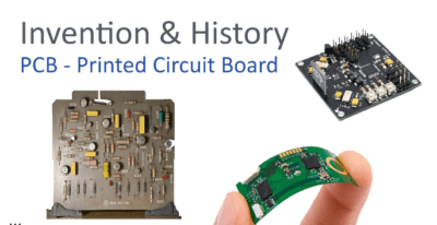
An Introduction to Printed Circuit Boards
An Introduction to Printed Circuit Boards Electronic gadgets saturate the cutting-edge world. Whether it’s for a tool that silently video displays units’ vitals or a phone with a limitless circulation of notifications, all incorporate a PCB circuit board on the coronary heart in their layout.
Over the years, revealed circuit board production has persevered to develop for you to maintain up with the growing needs of newer, faster, and greater complicated digital circuitry. Lead Free PCB Assembly Discussions on the techniques worried in devising and designing a PCB circuit board should fill a library, however right here we can offer a surface-degree advent of the basics.
- What Is a Printed Circuit Board?
A revealed circuit board is an inflexible shape that includes electric circuitry made of embedded steel surfaces referred to as strains and large regions of steel referred to as planes. Components are soldered to the board onto steel pads, that are related to the board circuitry. This lets additives be interconnected. A board may be composed of 1, or more than one layer of circuitry.
Circuit forums are constructed with a dielectric center fabric with bad electricity engaging in residences to make sure natural circuitry transmission and interspaced with more layers of steel and dielectric as wanted. The wellknown dielectric fabric used for circuit forums is a flame-resistant composite of woven fiberglass fabric and epoxy resin, referred to as FR-4, even as the steel strains and planes for the circuitry are commonly composed of copper.
- Board Class
Printed circuit forums are used for a lot of purposes. One distinguishing feature of PCBs is their magnificence–both 1, 2, or three. The magnificence of PCB shows its normal reliability and great layout.
Class 1 forums designate a purchaser digitally.
Class 2 forums are determined in gadgets wherein excessive reliability is important, however now no longer crucial. These gadgets try and reduce failure.
Class three forums constitute the maximum exacting production requirements of a PCB. Simply put, if a Class three board fails, lives are right away at stake–for example, the forums on an airplane.
- Types of Printed Circuit Boards
In general, forums may be classified into certainly considered one among 3 categories: inflexible, flex, or steel-center forums.
FR-4
Rigid forums are regularly the considerable majority of forums a clothier will encounter, wherein the format of the board is contained inside an inflexible substrate made out of an excessive warmth and strain lamination process. The not unusual place fabric for those forums is FR-4, however relying upon the precise desires of the layout, this could be changed to emphasize or in any other case enhance positive traits of the board.
Flexible forums are composed of a much less inflexible fabric that lets in a long way extra deflection. The fabric is tactilely paying homage to a movie role, and the board thickness is commonly a long way much less than a wellknown inflexible board. While they’ve already been visible in a few usages, there’s a wish that bendy forums will usher withinside the subsequent step of wearable generation and eliminate the modern planar constraints inherent to inflexible board gadgets.
Metal-center
Metal-center PCBs are something of an offshoot of inflexible board designs, with a multiplied cap potential to burn up warmth at some point of the board to defend touchy circuitry. This fashion may be a choice for excessive-modern designs to save you thermal put-on and failure.
Wherever managed electromagnetism exists, revealed circuit forums shape the infrastructure to keep it. Of course, circuit forums don`t simply spring out from nothingness–their layout and production are a big engineering project unto themselves.
- The Process of Printed Circuit Board Design
Before a broadcast circuit board may be constructed, it should be designed. This is completed with the use of PCB circuit board layout CAD equipment. PCB layout is damaged into important categories: schematic seizes to create the circuitry connectivity in a diagram after which PCB format to lay out the real bodily circuit board.
- Develop the Library CAD Parts
The first step is to increase the library CAD elements wanted for the layout. This will encompass schematic symbols, simulation fashions, footprints for PCB format, and step fashions for the three-D revealed circuit board display. Once the libraries are ready, the subsequent step is to create the logical illustration of the circuitry on a schematic. CAD equipment is used to area the symbols on a schematic sheet after which join them collectively to shape the circuitry.
At the identical time, circuit simulation is administered to confirm that the layout will paint electrically in the manner it’s far supposed to be. Once those obligations are completed, the schematic equipment will ship their connectivity statistics over to the formatting equipment.
- Layout
On the format facet of Mad PCB layout, the schematic connectivity is acquired and processed as nets that join or greater thing pins collectively. With a definition of the supposed board form at the screen, the format clothier will area the thing footprints in the perfect locations.
Once those additives are optimally organized, the subsequent step is to attach the nets to the pins by drawing the strains and planes among the pins.
The CAD equipment can have layout guidelines constructed into them that save you the strains of 1 internet from touching every other internet in addition to governing many different widths and areas wanted for an entire layout. Once the routing is complete, the layout equipment is used once more to create production drawings and the output documents that the producer will use to construct the board.
The layout and production of a circuit board is a step-through-step process: schematic advent and simulation, putting in PCB layout grids and DRCs, thing placement, PCB routing, energy planes, and sooner or later assembling the BOM and constructing the board. The subsequent level of layout will recognition in those steps. An Introduction to Printed Circuit Boards